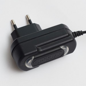
 I found an old GSM charger and I wondered if I can use it for something. On the label it sais 4.8 to 8.5V. What a precision! And if you wonder – it’s not within spec – the output is 9.5V.
Well let’s open it and see what’s inside.
Surprise!!! A killer device:
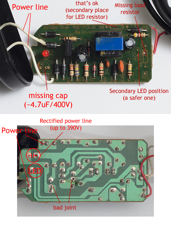
Why is this device dangerous? Check the position of the LED – it’s between the 2 power line tracks. Also it’s near the filter cap which could go to 390V DC. This tiny little space between tracks is not enough to ensure safety. And if you look at the charger photo you will see that they can use one of two positions for LED. One in the low voltage part, the other in high voltage part.
Now about the quality. Let’s just ignore the fact that schematic is really bad. It looks like some kind of buck regulator with no feedback from the output (yes, it’s not flyback). But let’s pretend the schematic works just fine. Why did they skipped the input filter capacitor? That’s going to make output ripple higher than the output voltage :). Well I forgot to measure the output ripple before I fix it and now I’m too lazy to remove those parts again. And surprisingly they put 4 diodes – full wave rectification. Usually they skip 3 and put only one. I guess they couldn’t make it work without cap and 3 diodes so they decided to put some “extra” parts. And they think they did smart thing because probably diodes are cheaper than the capacitor.
So here is what I did to make it safer:

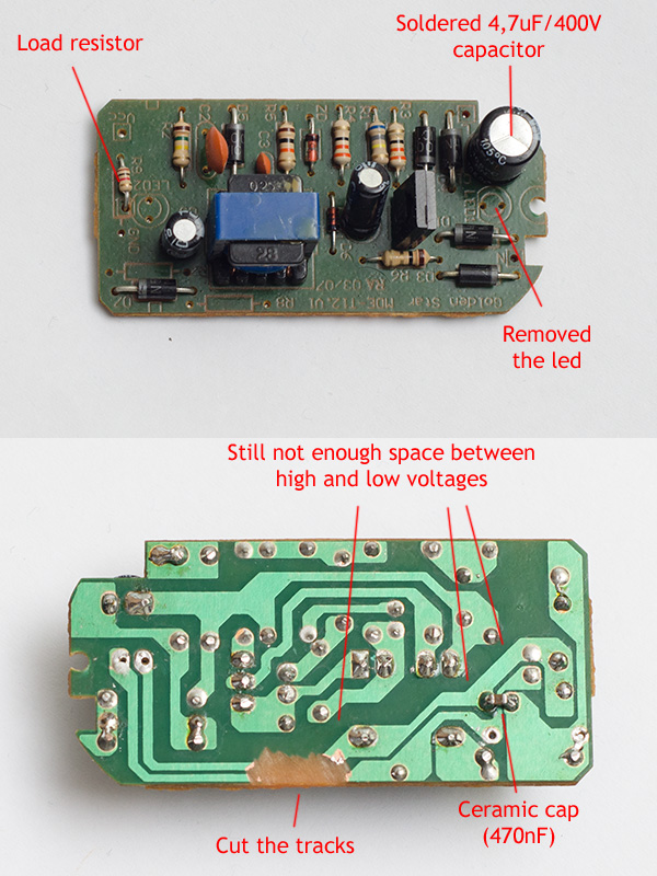
I’ve soldered a high voltage 4.7uF capacitor after the bridge rectifier. I fixed the bad joints. I also soldered a ceramic capacitor in the output to reduce ripple voltage. I could also change the output 100uF capacitor with a good low ESR one because the original one is probably not low ESR, but I don’t need that low ripple. I’ll use it for digital stuff only. I removed the led and replaced it with 1k dummy load resistor to avoid high voltages on the output. You have to be careful when
So what’s the conclusion? It’s not

